Advertisement
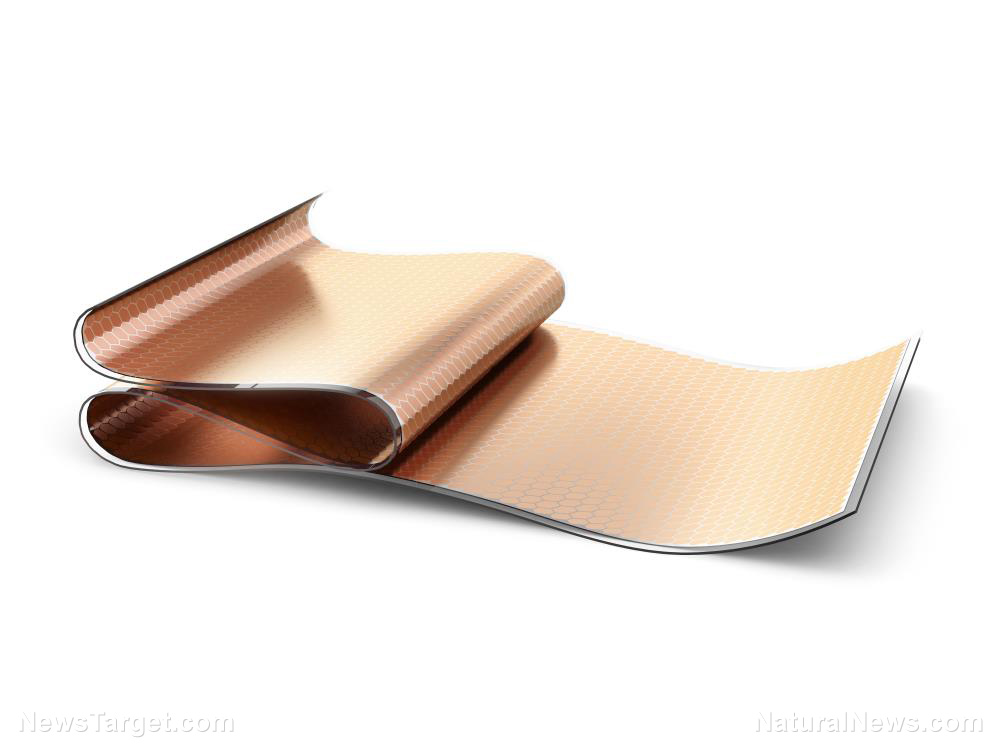
Three-dimensional materials have finally reached the peak of their performance. Electronics built out of these legacy semiconductors can no longer be made any smaller, stronger, and more efficient at the same time. So researchers are working on 2D nanomaterial replacements that can meet these insatiable demands.
The conventional 3D semiconductors enjoyed a good run that lasted for 60 years. They were successfully shrunken down to create microelectronics. Every molecule, every atom, and the spaces between those particles were exploited for storing data or energy. And their performance was pushed to the physical limit of efficiency.
However, all good things have to come to an end. The current generation of electronic devices can no longer be scaled down and made more efficient at the same time, not if they are using the traditional materials.
Compromises must be made. A device can be made even smaller, but it will run slower or have a shorter operational time. Conversely, its energy efficiency can be improved, but it will be bigger or run slower than desired. Or it can run for long periods of time, if you are fine with the processing power of an electronic watch. (Related: New “smart” fabrics will allow you to wear your electronics.)
2D materials are taking over the roles of 3D semiconductors
University of Pittsburgh (Pitt) assistant professor Susan Fullerton is one of the many researchers who are investigating alternative semiconductors for the next generation of electronics. She developed 2D materials that are no thicker than a single molecule.

Fullerton said that traditional semiconductors can no longer handle the requirements of the latest computing processes. They are not fast enough to respond within nanoseconds, incapable of operating at sub-volt levels of power, and can only offer a fraction of the 1,000 unique resistance states required by machine learning.
With those requirements in mind, she explored the potential of using ions in electronics. Many studies have established that ions could manage the passage of electric charges through very thin semiconductors with great efficiency. This property made lithium-ion a valuable material for many electronic devices.
Fullerton designed a multi-layer stack of 2D semiconductor sheets. This arrangement of ultra-thin materials would expand the space for storage, will use less power, and greatly increase processing speeds.
To power this arrangement, she and her Pitt colleagues created a “monolayer electrolyte.” This material contains plenty of ions. Furthermore, it matches the single-molecule thinness of the semiconductor sheets.
Mixing ions with 2D materials is risky but very promising
Fullerton pointed out that the semiconductor industry has avoided this path of technological development for a reason. Unlike ordinary semiconductors, ions must be strictly controlled at all times.
“Ions are often ignored because if you cannot control their location, they can ruin a device,” she said. “So the idea of using ions not just as a tool to explore fundamental properties, but as an integral device component is extremely exciting and risky.”
Still, she believed the rewards are well worth the risk. Fullerton said that the industry desperately need new materials with the right kind of physics and properties that could break free of the current constraints on size. Therefore, the combination of high-powered ions and 2D materials could potentially get adopted for the next generation of high-performance computing devices.
The National Science Foundation seems to share her opinion. The federal agency recognized their accomplishments with an award and a cash grant.
Fullerton will invest the reward into improving the prototype monolayer electrolytes. In addition to creating the next generation of semiconductor materials and electronics, she is also reaching out to students who could become the next generation of electronic materials researchers.
Sources include:
Submit a correction >>
This article may contain statements that reflect the opinion of the author
Advertisement
Advertisements


